Real-Time Debugging
Highly Integrated Embedded Wireless
Devices
David
Ruimy Gonzales, Senior Member of Technical Staff
Brian
Branson, Design Manager
Motorola M•CORETM
Technology Center
Introduction
Highly integrated wireless
solutions continue to increase in demand, as silicon providers respond with a
broad array of intellectual property, increasingly dense technologies, and an
industry-wide focus on System-On-Chip (SOC) design tools and integration
methodologies. The trend toward reducing the number of components in these
systems clearly has the advantage of reducing cost, overall power consumption
and manufacturing complexity.
On the other hand, product
developers are left with the daunting task of realizing complex devices with
increasingly reduced visibility of subsystem interaction. These devices use
programmable microcontroller (MCU) and digital signal processor (DSP) cores
coupled to embedded memories and a myriad of peripheral modules on a single
chip. This trend toward more highly
integrated systems clearly is increasing the need for improved methods of
system validation.
SOC design methodologies for
programmable cores now include static debug blocks, which may be used during
the early stages of product development.
By including additional debug related capability on-chip suppliers are
offering designers the ability to fully understand the behavior of a given
system, including validation of both hardware and software architectures, and
their interdependence. This is essential for evaluating real-time power
consumption in Internet ready handheld devices.
This paper explores the
issues associated with developing power efficient handheld wireless devices and
the necessary on-chip debug capability needed for rapid product development. Debugging highly integrated multiple core
systems on a single chip will be discussed using the M•CORE M341 micro-RISC
processor as an example. An
implementation of a real-time debug port based on the IEEE Industry Standards
and Technology Organization (ISTO) Nexus 5001 ForumTM specification
will also be discussed.
Understanding
Embedded System Behavior – Power Profiles
To better appreciate the problems in developing a low
power/high performance system, a cellular handset may be a good place to start.
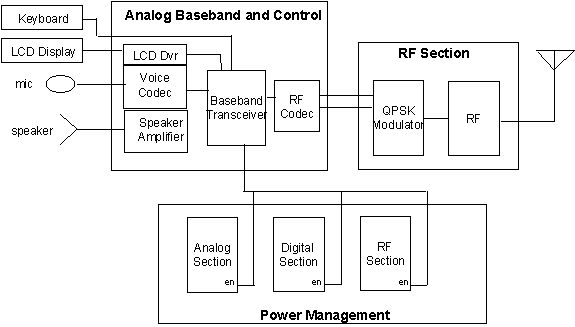
A digital cellular handset can be
partitioned into 3 main sections as illustrated in Figure 1. The RF section receives and transmits analog
and/or digital information, the Analog Baseband and Control section handles
intermediate frequency conversion, user interaction and power control, and the
Power Management section distributes and manages power to all elements of the
handset.
Figure 1 – Digital Cellular Handset Block Diagram
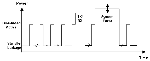
In first and second generation digital cellular
solutions, overall baseband power consumption is derived from the combination
of 1) standby leakage power, 2) active
power for time-based protocol software stacks & data (voice) transmission,
and 3) system event power induced by an active page or call, or other user-induced
event as illustrated in Figure 2. The relative periods of standby and active
power can be calculated with decent accuracy based on knowledge of the wireless
protocol. Standby power consumption can
hence be estimated via leakage current information for a given technology, and
knowledge of the amount of time the chip stays in this inactive mode.
Active power consumption is a
bit more difficult to estimate, but for repetitive software stacks performing
known protocol functions, this too can be relatively accurately
determined. Consider then the problem
of estimating and optimizing on-chip power consumption during user-induced
events such as Wireless Application Protocol (WAP) browsing, high-speed down/up
link transactions, Motion Picture and Entertainment Group (MPEG4) structured
audio activity, etc.
Figure 2 – Characteristic Power Consumption for Cellular Handset
The embedded system contains all the necessary
capability to perform these functions, even in parallel with other events, but
their behavior is much less deterministic.
Software written to handle this multitude of
system activity must be carefully optimized to improve overall battery life for
a particular application. Prior
studies show that the three main blocks of the cellular handset each consume
from 15 to 50 milliamps (ma) of current depending on its state of activity as
illustrated in Table 1.
Table 1 – Cellular Handset Power Consumption
|
Task |
Digital Power |
Analog Power |
RF Power |
|
Network Access |
40ma |
20ma |
40ma |
|
Call Service |
20/30ma |
20ma |
50ma |
|
3G Playback |
35 ma |
15ma |
50ma 20/30ma |
Real-Time Performance
Analysis is Changing
Lab bench analysis of
prototype systems permits conventional methods of evaluation such as circuit
boards with logic analyzer interfaces.
Typically these boards provide a means for initial power up and
integration of software and hardware modules.
Each core in the baseband processor chip is evaluated individually in a
static debug form where they are each put in a special mode of operation and
their programmer model registers and memory are checked while single stepping a
test program which was downloaded from a host computer. Once the system passes the “smoke test” where
each processor exits reset and performs initialization functions correctly, the
task of debugging real-time kernel and interrupt structures begins.
The art of debugging a
real-time wireless device has classically required the use of a logic analyzer
monitoring an external bus interface where at each clock cycle a sample of bus
activity is recorded. This is becoming
extremely expensive and physically impossible as microcontrollers and DSPs
operate above 100mhz.
When bus interfaces are not
available developers embed “printf” statements in their code at strategic
points so data needed is sent to a peripheral port and retrieved by a host
processor. The information is minimal
and presents intrusive delays in the application. This has become unacceptably time consuming as system software
layers become more complex. This being
a common problem, microcontroller developers are now demanding reliable and
cost effective solutions from semiconductor suppliers and development tool
vendors.
IEEE-ISTO Nexus 5001 ForumTM
addresses Real-Time Debugging
Over the past two years a consortium of companies has
diligently worked to address the issue of real-time debugging highly embedded
systems. The automotive,
telecommunications and the network appliance industries have driven this effort
to reduce time to market of new products.
The consortium began with 5 companies and has grown to over 25 companies
actively participating in the definition of a specification, which is now governed
by the IEEE-ISTO Nexus 5001 ForumTM.
The objective of the IEEE-ISTO Nexus 5001 ForumTM
is to define a common set of microcontroller on-chip debug features, protocols,
pins and interfaces to external tools which may be used by real-time embedded
application developers. At this time revision 1.0 of the specification is
currently available for review and serves as the model for future on-chip debug
resources implemented by silicon vendors.
One major objective of the forum is to help
development tool vendors more easily provide a standard set of tools, which may
be used on a number of embedded microcontrollers. In the spirit of reusability,
it has been recognized that many semiconductor vendors currently have debug
ports and tool sets that sufficiently address the static debug requirements of
their architectures. Providing a cost
effective yet powerful migration path to a standard set of dynamic debug
features is a key goal of the forum. More than 70% of leading embedded
microcontroller vendors have dedicated circuits and pins, which assist in new
product development based on the IEEE 1149.1 Joint Test Action Group (JTAG) 4
wire serial interface.
The JTAG pins and protocol help developers with
static debug methodologies in a master-slave mode but there is no means for the
embedded microcontroller to initiate real-time information transfers to a host
computer. The Nexus standard addresses this need with a scalable set of
features whereby existing debug blocks may be used with an extensible auxiliary
port. The features associated with this
new auxiliary port focus on real-time transfer of information to and from the
embedded microcontroller.
To address various levels of
development needs the Nexus 5001 Forum has categorized static and dynamic debug
features according to class levels.
These classes provide a means for implementing a scalable debug
architecture, which can address different market segment requirements. Also, it should be noted that when a product
is in development, it is desirable to have as many debug features available as
possible because of time to market constraints. Once a device is put into production however, it may not be
necessary or desirable to have all the development features and pins. Cost savings may be realized by implementing
a scalable debug port, which meets only the requirements needed for specific
stages of the product life cycle.
Embedded System Performance Considerations
As previously
illustrated, the heart of the cellular handset is the baseband transceiver,
which performs all computations relative to call service, Internet web
interaction and handset control. Figure
3 shows a block diagram of a Motorola wireless baseband processor, including
separate MCU and DSP core complexes, interfaced to separate on-chip RAM and ROM
memories and core-specific peripheral and I/O functions.
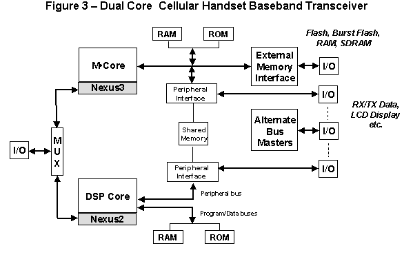
In order to fully understand each
cores’ operation separately, as well its interaction with the other, it would
be inherently desirable to pin out the internal core buses to external pads,
thus achieving good visibility of core bus cycles. However, due to the desire to reduce I/O and package costs, this
becomes prohibitive. Nonetheless,
system hardware and software architects still desire a method of understanding
standalone and integrated core behavior.
Hardware Requirements for
Supporting WAP Debug
Rather than elaborate on the details of the IEEE-ISTO
Nexus 5001 Specification, lets evaluate some of the needs of debugging an
Internet ready handset. The WAP
architectural specification focuses on optimizing for efficient us of device
resources. But the task of providing a communications protocol as well as an
Internet protocol layer dictates that the RAM required would be 1-4 megabytes
and the Flash ROM, which will hold the kernel, will be on the order of 256-512
kilobytes.
Since the number of external accesses to RAM directly
affects power consumption, the microcontroller engine must have an efficient
instruction set and resident cache and Memory Management Unit (MMU) to reduce
external bus transactions as illustrated in Figure 4. A key power consumption goal is to write the handset code so that
it efficiently uses the cache.
Once the cache and MMU are enabled, the interaction of
the core with the cache is no longer visible to the user unless there is a
cacheable instruction or data miss resulting in an external access to fill the
cache. This problem is aggravated when developers must debug code which
exhibits abnormal behavior in real-time or there is a need to capture power
measurements when running specific code.
Figure 4 – M•CORE M341 Processor with Nexus 5001 Debug Port
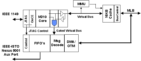
The M•CORE M341 architecture implements a Nexus 5001 port
for accessing user resources using a high speed output port to transmit
real-time program and data information.
The feature set of the Nexus 5001 port is of class 3, providing static
debug capability and real-time process identification, program trace, data
trace, and read/write access to M•CORE Local Bus (MLB) resources. The task of reporting real-time 32-bit
address and data values through a 2 to 8 bit output port requires that an
efficient method of transmission be utilized.
Applying Real-Time Features
Using Public Messages
A set of data packets, commonly referred to as Public
Messages in the Nexus 5001 specification, has been defined for efficient
transfer of debug information between the embedded processor and a development
system. Public Messages consist of a
transfer code or TCODE, source processor identification number, and the data
associated with the particular feature being accomplished. A key requirement in the definition of the
Public Messages is efficiency; thus packets may be variable in length depending
on the TCODE.
Messaging capability is controlled by a JTAG serial
interface. The JTAG interface couples
to a OnCETM static debug block and provides access to all Nexus 5001
registers on the M•CORE M341 processor.
Messaging capability is enabled prior to desertion of the reset pin so
exit from reset may be monitored.
Monitoring Program Flow
Following program behavior
can be reduced to the changes in the program counter due to branching, jumping
to subroutines and servicing interrupts and exceptions. Analysis shows that on average 12-13%
of instructions executed in a program
are of change of flow nature. Therefore, it is not necessary to report every
instruction’s address but rather only report the change of flow. What is needed to follow the source listing
is where you are relative to a reference start address, and where you are going
when you change program flow.
Three types of public
messages provide program flow behavior. Real-time operating system (OS) debug
must have a means for reporting a process ownership identifier. The objective
of the Ownership Trace Message is to give the most current value of the data
bus when a process writes to a special address. This address is called the User Base Address where comparators on
the Nexus 5001 snoop logic triggers a capture of the data bus. Thus, whenever a context switch of the OS
occurs, a process identifier may be transmitted using Ownership Trace message. This may be key for correlating virtual to
physical address maps of the MMU when sending messages to the source level
debugger.
Branch Trace Messages report when direct branch or
indirect branch instructions are executed.
The difference in the messages is that in a direct branch occurrence,
the only information needed is the number of instructions executed since the
last change of flow. A reference
address using a Sync Message is normally transmitted to establish where the
program counter currently is. After
that, all references are made to that address until an indirect change of flow
occurs. This reduces the number of bits
transmitted in a message. Indirect
branch messages report the number of instructions executed since the last
change of flow and the address where the program counter is jumping to, thus
establishing a new reference address.
If you need to report specific memory accesses, the
Watchpoint Message does the job. This
message triggers off hardware comparators and complex access qualifiers, which
monitor the M•CORE virtual bus.
The idea is to set a watchpoint trigger where a
signal as well as a message may be transmitted. The message tells which of the watchpoint triggers occurred. This is especially valuable for debugging variable
writes. For example, if you have a
global variable, which is being modified by a number of processes, and you want
to pinpoint which of those processes is accessing that variable, the watchpoint
message is the tool to use. This
feature also asserts an event out pin, which may trigger a logic analyzer to
capture specific public messages and/or peripheral signals. For power analysis, the trigger may be used
to capture current measurements at specific points in code or data accesses,
which may be useful for pinpointing power consuming hot spots.
Monitoring Data Variables
Data Trace messages provide a means for reporting
real-time data accesses to memory locations. Reporting data loads and stores
has a much higher instance than reporting program flow changes. Analysis has shown that as much as 25% of
instructions executed in a program are data accesses. Data Messages may be used
to report stack contents, global and local variables as well as peripheral port
accesses. To control the number of
Data Messages transmitted data trace qualifiers include the access type, i.e.,
read/write or either, as well as a start and stop address range. If the data address and access type
qualifiers are met, data messages are generated and sent to the debug
port. This narrows the window of memory
locations, which may incur a Data Message.
Only sending the unique portion of the data address
instead of the complete address reduces output bandwidth requirements for the
debug port. Consequently a data trace
message is reconstructed relative to each prior message using a synchronization
message as a reference address to begin with.
Real-Time Data Access
Capability
The M•CORE M341 Nexus port
provides access to the MLB mapped resources via the JTAG port. A Ready for Transfer pin (RDY) was added to
increase the transfer rate.
Calculations show that accesses to the Read/Write Data Register allow
for a throughput of 1 megabyte per second on an M•CORE M341 microcontroller
operating at 50 MHz system clock. Block
transfers are possible with a single setup of Read/Write control and address
registers. This permits 32 bit
transfers in 38 JTAG clocks where each JTAG clock is one-half of the system
clock.
This capability
significantly reduces program and data load times as well as enables the
developer to examine arrays of memory without stopping the application. Data Trace Messages only report data
movement within a well-defined data window while Read/Write Access permits
accessing values asynchronously. This
feature is very useful for downloading new filter coefficients or encryption
keys when testing communication protocols.
Another important use is the retrieval of power data values, which may
be built into the power management unit of the handset.
Real-Time Debug Tool Support
Two key ingredients to
successfully reducing development time is on-chip circuits such as the Nexus
5001 port we just described and the development tools which support the Nexus
interface. The Nexus 5001 specification
defines pins, connectors and the protocol for transferring messages to and from
the host computer. However, it is very
difficult to define stringent rules for Nexus register sizes, bit positions and
other implementation specific details, which may not suit particular
semiconductor vendors’ architectures.
An application protocol interface (API), which abstracts implementation
details, is the ideal solution for tool vendors.
Figure 5 – Real-Time Debug
Environment
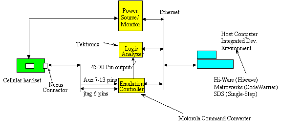
Figure 5 illustrates a lab
debug environment, which uses an integrated software tool set coupled to a
logic analyzer and power source/monitor for complete handset development. The emulation controller provides the
abstraction layer so that an API may be defined which provides the details at
the emulation controller to Nexus interface without burdening the Tool Vender. An FPGA was added to the emulation
controller, which would reconstruct the full message from the two Nexus port
output pins to a 40 bit wide message with message trigger signal. This improves utilization of the logic
analyzer’s trace buffer.
Classical debuggers use a
load, arm, go scenario where once the debugger has sent the target processor(s)
to work, the debug environment is frozen until the target processor re-enters a
debug or interrogation mode. To fully
exploit the real-time debug capabilities of the M341 Nexus port, the debugger
must permit interrogation of target resources as it executes code in
real-time.
Figure 6 – Hiware’s Hiwave Debugger and Tektronix TLA714 Trace Buffer
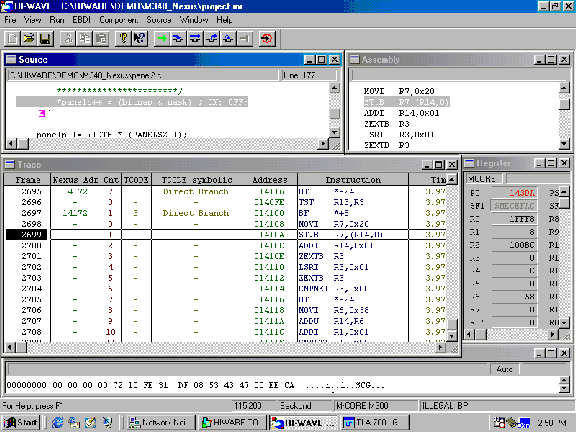
During initial development of
the M341 Nexus port, a Hi-WARE (Hiwave) debugger was interfaced to a Tektronix
TLA-714 logic analyzer. The Hiwave
debugger directly interacts with the Tektronix logic analyzer to arm its trace
buffer for message captures and later displays the trace buffer contents within
the Hiwave environment as illustrated in Figure 6.
Since the M341 processor has
a different instruction set and programmer’s model than the DSP56600
architecture, a dual integrated environment with split windows, one each for
the respective processor is utilized for debugging the baseband
transceiver. A single emulation
controller is used which can communicate with each processor using the JTAG
protocol. A semaphore configuration in
the dual debugger’s control module regulates traffic to the emulation
controller so there are no message collisions when communicating with either
processor.
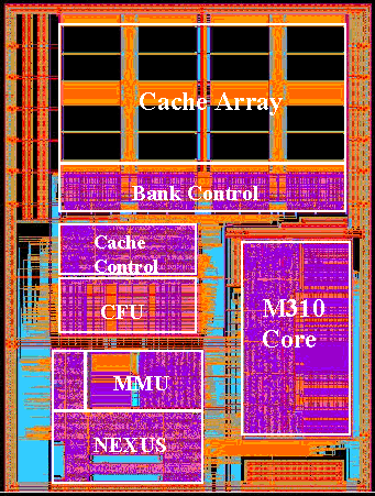
Figure 7 – M•CORE M341
Processor Die Photo
Real-Time Debugging
Penalties can be Minimized
The additional feature set
of the Nexus port doesn’t come without some die area and power penalty. Therefore, during its implementation all sub
module clocks were gated off for inactive circuitry and the message decode
state machine and logic were enabled/disabled via Nexus control. Special consideration was given to the
message queues to reduce power and the output port was made variable width to
accommodate a 2 or 8 bits width. This
is quite important from a development perspective. During lab analysis the 8-bit port would be used since there was
room to add larger connectors on the evaluation cards. But once the handset ergonomics had been
finalized and the high-density double sided surface mount board was used, it
was decided that a reduced bandwidth over the output port could be feasible at
that point in system development.
Overall the Nexus Class 3 implementation was 7.5% of the M341 processor
area as illustrated in Figure 7. But
considering the size of the complete baseband transceiver, it becomes quite
small relative to the addition of on-chip memories and the DSP.
SUMMARY
Cellular based products, which can interact with the
internet, are growing at a phenomenal rate.
This increase in features will lead to more sophisticated portable
systems and will challenge designers to provide more features at less power
consumption. Therefore system
validation will play a more important role in SOC design methodologies in order
to meet short time to market cycles.
Significant effort is underway throughout the
electronics industry to improve tools and methods for designing complex
embedded systems. The IEEE-ISTO Nexus
5001 Forum is a testament to this and demonstrates that there is a dire need to
standardize on a set of features, protocols, pins, interfaces and tools for
rapid development of real-time microcontroller based products.
Originally targeted for automotive applications, the
Nexus 5001 Forum has extended the scope of this effort to encompass
telecommunications, industrial and portable hand-held products. The problems of real-time visibility to
deeply embedded microcontrollers are very similar if not identical to most
product types. Each will have special
cases for solving specific design issues but the proposed global standard has
addressed this by allowing for vendor defined blocks for special features, all
addressed by a common protocol.
Feedback and comments as well as the full specification may be
downloaded at Internet web site <www.ieee-isto.org/Nexus5001/index.html.>
M•CORE and OnCE are
trademarks of Motorola. All others are
trademarks of their respective companies.