PIC Module
For
Reprogrammable
Flash Microcontroller
S Gupta
Summary
This articles discusses
the construction of PIC Module, which can be used for MicroChip Technology’s
reprogrammbale PIC16F873/6 Flash microcontroller. Schematic diagram is provided
and some of the features of flash microcontroller are highlighted with an
emphasis on flash memory reprogramming.
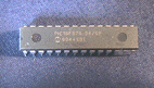
PIC16F873 Flash Microcontroller
Feeding on the success of PIC16F84, Microchip Technology’s PIC16F87X series of microcontrollers are destined to make a major impact over 8-bit reprogrammable microcontroller arena. PIC16F87X microcontrollers are built on the popular 14 bit PIC16C core and offer significant improvements over earlier cousins. As this microcontroller module uses only 28 pin devices (PIC16F873 & PIC16F876), only these devices are discussed in context of this article. Some features of these devices are highlighted below.
Memory
16F87X microcontrollers carry a large memory array, which can be divided into three types
- Flash Program Memory
- EEPROM Data Memory
- Data RAM (SRAM)
Flash Program Memory
The entire program memory is made up of flash array. Every single byte of flash program memory can be erased and reprogrammed. This can be done either in a conventional PIC programmer such as economical PICSTART units available from Microchip, or can even be done during an application. And all this can be done by a small user code resident in program memory, without requiring any external higher programming voltage. This level of flexibility is very beneficial in todays fast pace development, where product updates and modifications are routinely carried out in the field.
Reading and writing to program memory through user code is done through a set of special function registers (SFRs). The program memory is not limited to storing code bytes, but can also be used to store 14 bit of coefficient constants. An accidental access to an invalid code byte will result in execution of NOP code, without causing any harm. But unfortunately, it cannot be relied upon and care should be taken to ensure that any coefficient bytes are not accessed as program code bytes.
The lower of the two devices PIC16F873 has 7168 Bytes (4096x14 Words) of code memory while the other device PIC16F876 has 14336 Bytes (8192x14 Words) of code memory.
EEPROM Data Memory
EEPROM data memory is suitable for multiple erase and write operation. This is normally suitable for storing coefficient data, which may be programmed from time to time. The EEPROM data memory is not mapped in register file address space, but is mapped differently, and is also accessed through a set of SFRs. PIC16F873 contains 128 Bytes of EEPROM data, while PIC16F876 contains 256 Bytes.
Data RAM (SRAM)
RAM availability in microcontrollers is increasing steadily and PIC16F series is no exception. PIC16F873 contains 192 Bytes of SRAM, while PIC16F876 contains a much larger 368 Bytes. The Data memory is partitioned into 4 banks of 128 Bytes each. The lower section (00 to 20H) of each of these banks is devoted to special function registers, and the balance is left for Data RAM. Since PIC16F873 only contains 192 Bytes of Data RAM, these are all contained in the first two banks. Only SFRs are located in the upper two banks bank 2 & bank 3. For PIC16F876 microcontroller containing 368 Bytes of Data RAM, these are spread in all four banks. This device has an interesting feature that the top 16 Bytes of each bank are used to address the same data memory space (70 to 7FH). This reduces the need for bank switching (a real nuisance)
Peripherals
PIC16F87X contains a rich set of on-board peripherals. These include
- A/D Converter
- Timers/Counters/PWM
- SCI
- IIC/SPI
A/D Converter
A/D converter resolution has been improved from standard 8-bit to 10 bit. This is reasonably good, and 16F87X microcontrollers can vie for a place in industrial control. 5 10-bit A/D channels are provided. The conversion rate can be adjusted internally, but for 10 bit results, a conversion time (including sample and hold) of 20 usec is optimum. Some of the analogue input channels can be configured as digital I/O, if all five channels are not needed. It is also possible to use an external precision reference voltage, but is generally an overkill for this resolution.
Timers/Counters/PWM
Accurate counting and timing circuits are becoming a necessity for modern industrial control. There are three timers on-board, which can also be configured to operate as counters.
- 8-bit Timer0
- 16 –bit Timer1
- 8-bit Timer2
Timer2 is supported by a period register as well as prescaler and a postscaler. This makes the timer operation very flexible. The timers are shared by two capture/compare functions as well as PWM output. PWM resolutions of up to 10-bits can be achieved. Capture resolution is claimed to be 12.5 nsec at 20 MHz clock operation (very impressive), and compare resolution is 200 nsec.
SCI
There are a number of programs written to set any I/O pin of a PIC microcontroller to act as a software-UART. Yet, a software-UART does not offer the type of response needed for real time control. It is especially true, if the microcontroller is connected in any sort of communication network, where data is constantly flying through the interface. A high speed hardware UART is built in PIC16F87X microcontroller. It has its own dedicated baud rate generator, allowing flexible baud rate to be generated. The choice of a suitable crystal is necessary to achieve reliable operation at high baud rates such as 115K.
IIC / SPI
There has been a recent surge in devices offering IIC and/or SPI interface. Majority of these devices are EEPROMs or data converters. A synchronous interface is provided, which can be set up either for IIC or SPI communication. These interfaces can also be used for a small scale local area network between a PIC working as a master controller and several other units working as slaves, in close physical proximity.
Besides these functions PIC16F87X microcontrollers contains several other peripheral functions, such as watchdog timer, power on reset, brown out reset and sleep mode.
Reprogramming Flash Program Memory
Flash program memory can be reprogrammed either through in-circuit serial programming (ICSP) interface, or through a user program running in the device itself. It is generally a good idea to provide some sort of protection for accidental erasing of critical sections of code. PIC16F87X microcontroller also address this issue.
Program Memory Code Protection Bits
A PIC16F87X microcontroller can only be reprogrammed, if certain bits in the configuration register are in correct state. These bits are:
- CP1 & CP0
- WRT
CP1 and CP0 provide code protection for certain blocks of program memory. The following table lists the effect of these two bits on code memory.
Code Protection Bits - PIC16F873
CP1 |
CP0 |
Protected Code
Memory (Words) |
|
0 |
0 |
0000 – 0FFF |
|
0 |
1 |
0800 – 0FFF |
|
1 |
0 |
0F00 – 0FFF |
|
1 |
1 |
None. Entire memory can be modified |
Code Protection Bits - PIC16F876
CP1 |
CP0 |
Protected Code
Memory (Words) |
|
0 |
0 |
0000 – 1FFF |
|
0 |
1 |
1000 – 1FFF |
|
1 |
0 |
1F00 – 1FFF |
|
1 |
1 |
None. Entire memory can be modified |
WRT bit further controls the reprogramming of program memory through user code. For the selected block of code to be reprogrammed on a word (14 bit) basis, the WRT bit should be ‘1’. If, it is set to ‘0’, the user code cannot modify the program memory, it can be done through external ICSP interface.
All the three bits, even though are resident in code memory space (2007H), are not accessible to internal user program. To be correct, configuration register is located in a special test/configuration memory space and is not accessible to SFRs used in internal programming. The bits in configuration register can only be reprogrammed, after entire device is erased. Thus, the very first time, when the device is programmed the configuration bits have to be set appropriately, so that in circuit programming through either a user code or through ICSP interface can be carried out.
SFRs Used In Flash Programming
There are six special functions registers, which are used in reading and writing to flash program memory. These are:
- EEADR
It contains the low byte address of program memory location to be accessed
- EEADRH
It contains the high byte address of program memory location to be accessed. Since, there is a maximum of 8K words of program memory (PIC16F876), only a 13-bit address is required. Thus, only the lower (LSB) 5 bits are valid and the upper 3 bits are not used and will read as ‘0’.
- EEDATA
It contains the lower 8 bits of (a total of 14 bits) program word.
- EEDATH
It contains the upper 6 bits of program word. These bits are located in the lower 6 bits of EEDATH byte. The upper two bits of this register are not used and will read as ‘0’.
- EECON1
This is the main control register for programming flash memory as well as EEPROM data memory. Only 5 bits of the 8 bits are valid and the other three read as ‘o’. These bits are,
- EEPGD
(B7)
This bit dictates, whether program memory or data memory is being accessed
0 = Access data memory
1 = Access program memory
- B6: Unimplemented
- B6: Unimplemented
- B4: Unimplemented
- WRERR (B3)
This is a flag (status) bit and is used to indicate a error in programming. Programming of every single location is a timed event and any premature termination of this event may result in incorrect (or atleast unreliable) programmed data. Even though, user code can not prematurely terminate this event, it can be done through WDT or external MCLR reset.
0 = Location was programmed without interruption
1 = Programming was interrupted
- WREN (B2)
This bit enables the programming of program or data memory.
0 = Flash memory can not be written to (programmed)
1 = Flash memory can be written to
- WR (B1)
This bit is analogous to WR control line of a SRAM IC, but also acts as a status bit. The bit is set to program (write to) every single location (14 bit word for program memory and 8 bit of data memory). Once the programming of that location is complete, the WR bit becomes reset to ‘0’. This bit can only be set but not reset by user code. This is intentionally done to prevent a user code from prematurely terminating the write operation.
1 = Initiate a write operation (Acts as a control bit)
0 = Write operation is complete.(Acts as a status bit)
- RD (B0)
This bit is similar to RD control line of a SRAM. This bit needs to be set to carry out a read operation on program or data memory.
0 = Do not initiate a read operation
1 = Initiate a read operation
Program memory – Read Operation
Even though, the intent may be to write to (program) a memory location, memory reading is required to verify that programming has been carried out successfully. The data is normally read and is reprogrammed, if not suitable. Once a code location has been programmed, it is read to verify that programming has been successful. Every single program memory location (14 bit word) is read as two bytes of data. The read operation is as follows:
- Select register bank 2 to access EEADR, and EEADRH SFRs
- Transfer Upper and lower bytes of address to EEADRH (5 LSBits representing the 5 MSBits of 13 Bit address) & EEADR respectively
- Switch to Bank 3 to access EECON1 SFR
- Set EEPGD bit to select program memory
- Set RD bit
- Wait for two clock cycles
- Switch to bank 3 to access EEDATA and EEDATH SFRs
- Retrieve the data from EEDATA and EEDATH
Software: Read Flash Program Memory
; RAM Registers
; -----------------
; It is assumed that the address
bytes are properly set up
ADRSL EQU 70h ;
Low byte of EE Address
ADRSH EQU 71h ;
High byte of EE Address
DATAL EQU 72h ;
Low data byte
DATAH EQU 73h ;
High data byte
; Save bank info
SWAPF STATUS,W ;
Retrieve Status register
;
Do not affect flags
MOVW TEMP ;
Save Status register
; Select
bank 2
BCF STATUS, RP0
BSF STATUS, RP1
; Load
word address into registers
MOVLW ADRSH ;
Read high byte of address
MOVW EEADRH ; Load high byte of address
MOVLW ADRSL ;
Read low byte of address
MOVW EEADR ; Load low byte of address
; Select
bank 3
BSF STATUS, RP0 ; RP1 is already set
BSF EECON1,EEPGD ;Set program memory
as the target
BSF EECON1,RD ;Initiate
memory read operation
;
Include these two instructions as these will be read but not acted upon
; Essentially a time killing
proposition.
NOP
NOP
; Read
data from SFRs
; Switch
bank (2) to access EEDATA & EEDATH registers
BCF STATUS, RP0
MOVF EEDATA,W ; Retrieve low byte of data
MOVW DATAL ; Store low byte
MOVF EEDATH,W ; Retrieve high byte of data
MOVW DATAH ; Store high byte
;Retrieve bank info
SWAPF TEMP,W ;
Retrieve Status register
MOVW STATUS ;
Save Status register
RETURN
Program memory – Write Operation
PIC16F87X allows a single program memory location (word) to be programmed, without any need to erase it. Every program memory location (14 bit word) is written as two bytes of data- 14 bits to be precise. It is recommended that interrupts be disabled during the actual programming phase. Programming of every location (through user code) requires a very specific sequence of instructions to be carried out. Thus, it is inconceivable that a code word may be inadvertently programmed. The sequence to program a program memory location is as follows:
- Select register bank 2 to access EEADR, and EEADRH SFRs
- Transfer Upper and lower bytes of address to EEADRH (5 LSBits representing the 5 MSBits of 13 Bit address) & EEADR respectively
- Transfer Upper (6 LSBit representing the 6 MSBit of 14 Bit data ) and lower bytes of word data to EEDATH & EEDATA respectively
- Switch to Bank 3 to access EECON1 SFR
- Set EEPGD bit to select program memory
- Set WREN bit to allow program memory write (programming)
- Wait for two clock cycles
- Disable interrupts
- Write control code 55h to EECON2 SFR
- Write control code AAh to EECON2 SFR
- Set WR bit to the programming operation
- Do nothing for next two cycles
- Enable interrupts
- Reset WREN bit
- Switch to bank 3 to access EEDATA and EEDATH SFRs
- Retrieve the data from EEDATA and EEDATH
- Verify the data and reprogram if necessary.
Software: Program Flash Program Memory
; This subroutine will program the 14 bit of data into program
memory.
; It verifies the programmed data against the initial
data.
; If programming is successful, bit B7 of ERRCOUNT will
be set. The number tries are indicated ; by B1 & B0 of ERRCOUNT
; RAM
Registers
; ----------------
; It is assumed that the address
bytes and data bytes are properly set up.
ADRSL EQU 70h ;
Low byte of EE Address
ADRSH EQU 71h ;
High byte of EE Address
DATAL EQU 72h ;
Low data byte
DATAH EQU 73h ;
High data byte
ERRCOUNT EQU 74h ;
Error counter
; Save bank info
SWAPF STATUS,W ;
Retrieve Status register
;
Do not affect flags
MOVW TEMP ;
Save Status register
CLRF ERRCOUNT
AGAIN
; Select
bank 2
BCF STATUS, RP0
BSF STATUS, RP1
; Load
word address into registers
MOVLW ADRSH ;
Read high byte of address
MOVW EEADRH ; Load high byte of address
MOVLW ADRSL ;
Read low byte of address
MOVW EEADR ; Load low byte of address
; Select
bank 3
BSF STATUS, RP0 ; RP1 is already set
BSF EECON1,EEPGD ; Set program memory
as the target
BSF EECON1,WREN ; Enable memory write operation
BCF INTCON,GIE ;
Disable all interrupts
; Write
control bytes
MOVLW 55h
MOVW EECON2
MOVLW AAh
MOVW EECON2
;
Include these two instructions as these will be read but not acted upon
; Essentially a time killing proposition.
NOP
NOP
BSF INTCON,GIE ; Enable interrupts
; Read
data from SFRs
; Switch
bank (2) to access EEDATA & EEDATH registers
BCF STATUS, RP0
MOVF EEDATA,W ; Retrieve low byte of data
SUBWF DATAL ; Compare the programmed data
BTFSC STATUS,Z ; If both are same then check high byte
GOTO ERROR
MOVF EEDATH,W ; Retrieve high byte of data
SUBWF DATAH ; Compare the programmed data
BTFSS STATUS,Z ; If both are same
GOTO ERROR ; Both are not same.
BSF ERRCOUNT,7 ; Set bit B7
to indicate success in programming
;Retrieve bank info
SWAPF TEMP,W ;
Retrieve Status register
MOVW STATUS ;
Save Status register
RETURN
ERROR
INCF ERRCOUNT ;
Increment error counter
MOVLW 03H
SUBWF ERRCOUNT ; Is error counter = 3?
BTFSS STATUS,Z
GOTO AGAIN ; Try and program one more time
; No three tries have been made
and the byte is not yet programmed properly
; Exit after retrieving bank
info
SWAPF TEMP,W ;
Retrieve Status register
MOVW STATUS ;
Save Status register
RETURN
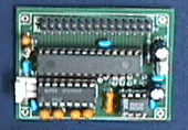
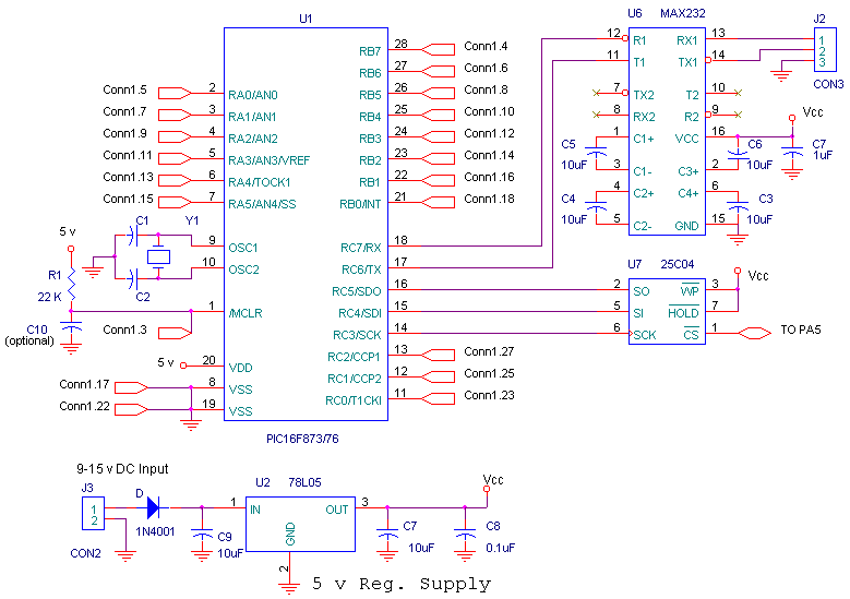
FLASH PIC Module
Click here for Flash Module Schematic Diagram
Flash module provides a compact target as well as development base for 28 pin PIC16F873 and PIC16F876 microcontrollers. All the external interface lines including, power supply, RS-232, and microcontroller I/O are brought to a dual inline connector on one side of the board.
Flexibility of I/O connector makes this module quite versatile. For very simple applications, the connector can be left out and wires directly soldered to the pc board. But, in general a connector offers more flexibility. User has a choice of two types of connectors: a right angle pin connector, and a straight pin connector. Right angle connector is useful for vertical installation in a target application. Straight pin connector is convenient for horizontal mounting of the module either on top or bottom of another interface board. It is also useful in situations, where the module is mounted on a flat panel surface and is connected to interface circuit through ribbon cable.
RS-232 Communication
A vast majority of microcontroller applications require a serial communication of some sort. An RS-232 voltage translator IC U2 (MAX232 or equivalent) provides the RS-232 interface. Only three interface lines RX, Tx, and Gnd are used. If for any reason, the module is going to be used in a stand alone application, without any RS-232 communication, these two I/O lines can be used for external interface. In this case, IC U2 need not be installed on the board.
A separate 3-pin header provides is provided in addition to the main interface connector. It duplicates the three interface signals Rx, Tx, and Gnd.
Power Supply
Microcontroller require a regulated 5 volt dc supply for proper operation. A 5 volt regulator (U2) is provided on –board. It requires an unregulated dc supply in the range of 8 – 12 volt. The unregulated dc is applied through the last two pins of main interface connector. The regulated 5 volt output is also available at the interface connector for driving low-power external circuit. Diode D1 protects against accidental reversal of power supply. If a regulated 5 v supply is available then, the 5 volt regulator circuit can be left out.
Clock Oscillator
PIC16F87X microcontrollers are available for operation at maximum frequencies ranging from 4 MHz to 20 MHz. A popular clock frequency is 4-MHz, which provides a time base of an even 1-microsecond; convenient in timing applications. Module has the provision to use either a ceramic resonator, or a crystal (with two capacitors). Resonator offers lower total cost but at the expense of reduction in timing accuracy. For precision timing, such required at high baud rates, it is recommended that a crystal be used.
SPI EEPROM
Even though the flash microcontroller contains reprogrammable code and data EEPROM, an external SPI-EEPROM can be installed on the Flash Module for data user storage. It is interfaced to PIC16F87X microcontroller through standard SPI interface pins. Interestingly, the interface does not have to use the hardware SPI facility of microcontroller and can still function using I/O pin manipulation (software SPI). The write-protect and hold functions of EEPROM are disabled by tying these to Vcc. The EEPROM is selected through port pin ‘PA5’. Any SPI device, external to Flash Module can still use the built in SPI interface as long as the on-board EEPROM is not selected (set PA5 to high). Any SPI-EEPROM (8 pin Dip) of desired capacity can be accommodated.
In the next issue a flash module will be discussed that can
be programmed, erased, and reprogrammed through serial port and tested in user
application. Say goodbye to PIC programmers.
For more information on Flash Module: email us.
![]()