ADuC812 MicroConverter
In a
Digital Storage Scope
S Gupta
Summary
This article discusses
the application of ADuC812 microcontroller from Analog Devices in a digital
storage scope (DSS). The operation of analogue to digital converter integral to
ADuC812 is discussed in detail. The article contains a complete assembly
language listing for implementing the DSS.
Analog To Digital Converter
ADuC812 contains a high-speed 12-bit analogue to digital converter (ADC) with a sample & hold, and an 8-channel analogue multiplexer. The conversion rate can be controlled through software but is limited to about 200,000 conversions per second for full resolution. A 2.5 volt low drift voltage reference is integrated on-board. If desired an external voltage reference capable of overdriving the internal reference can be substituted.
ADC Conversion Time
The ADC conversion relies on the internal ADC clock. This clock is derived from master clock MCLK, which is the clock signal generated through external Xtal. It is very important to select a proper ADC clock rate and it is recommended to set it between 400 KHz and 3 MHz. Any operation, outside this clock rate may result in a reduced performance. CK1 & CK0 bits in ADCCON1 control register control the ADC clock rate.
Table 1 ADC CLOCK RATE
CK1 |
CK0 |
MCLK Divider |
|
0 |
0 |
1 |
|
0 |
1 |
2 |
|
1 |
0 |
4 |
|
1 |
1 |
8 |
For an ADuC812 fed by 11.0592 MHz xtal, a minimum value of 4 should be used as clock divider. On the other hand, ADuC812 controlled by a 16-MHz xtal will require a clock divider value of 8. The minimum value of external MCLK is dictated by the minimum ADC clock frequency of 400 KHZ. Thus ADuC can be satisfactorily operated by a 400 KHz Xtal with MCLK divider value of 1. After the analogue signal has been captured by sample & hold, ADC takes next 16 clock cycles (ADC CLK) to complete the conversion
The ADC has a typical internal leakage of about 1 ma, with a maximum specified value of 10 ma. This is fairly large, when used to digitize signal from high impedance sources. It may become necessary to use an external voltage buffer, which can shield the high impedance source from the ADC leakage. The maximum source impedances that can be used in each case can be calculated.
Voltage reference = 2.5 v
Converter resolution = 12 bit
Converter resolution = 0.61 mv
Therefore the maximum source impedance: = 0.61 mv / Leakage Current in ma
· For 1 ma (typical) leakage current max source impedance = 610 Ohm
· For 10 ma (maximum) leakage current max source impedance = 61 Ohm
Even though, in majority of these devices (ADuC812) the leakage current will be limited to typical value, it is good engineering practice to prepare for the possible worst case scenario. An external op-amp configured as a unity gain buffer will practically eliminate the effect of leakage current. This op-amp should have a low offset voltage & bias current. It should also exhibit a low offset drift with variation in temperature. An added benefit of providing a front-end op-amp is that the acquisition time (in sample and hold circuit) is also slightly reduced. The internal sample and hold circuit carries a capacitive impedance of 20 pF (maximum)
Acquisition Time
As long as the source impedance is less than 610 W, or an external buffer amplifier is used, a minimum acquisition time equivalent to one ADC cycle is satisfactory. Otherwise the acquisition time need to be increased to compensate for the internal capacitor leakage current. The main drawback of increased acquisition time is the reduction in converter throughput, along with a reduction in the highest frequency component of input signal. The acquisition time is controlled by (AQ1 & AQ0) bits in ADCCON1 control register.
Table 2 ADC Acquisition Time
AQ1 |
AQ0 |
ADC CLK Cycles |
|
0 |
0 |
1 |
|
0 |
1 |
2 |
|
1 |
0 |
4 |
|
1 |
1 |
8 |
The ADC has a very flexible mode of operation. It can be operated in a single conversion or continuous conversion mode. The ADC conversion can be controlled by any one of the following:
- Software (User program)
- Timer2
- External Trigger (pin 23)
- DMA
Control registers ADCCON1 and ADCCON2 control the ADC operating mode. Both the registers can be addressed in direct addressing mode of 8051. Register ADCCON2 is bit addressable, while ADCCON1 is not. A third register ADCCON3 contains a single status bit ‘Busy’ (ADCCON3.0) indicating if ADC is busy doing the conversion. This bit is automatically cleared at the end of each conversion and set at the start of conversion. Conversion results are read from two 8-bit registers ADCDATAH and ADCDATAL. Register ADCDATAH contains four MSBits of result, as well as the channel setting for this conversion. The channel setting is located in the upper nibble and the lower nibble contains the four MSBit of 12-bit result.
Table 3 ADC Result Format
ADCDATAH
(Byte Register) |
Channel Selection Bits |
MS 4 Bits of Result (B11-B8) |
||||||
|
7 |
6 |
5 |
4 |
3 |
2 |
1 |
0 |
|
ADCDATAL(Byte Register) |
Lower 8 Bits of Result (B7-B0) |
|||||||
|
7 |
6 |
5 |
4 |
3 |
2 |
1 |
0 |
|
Software Control
The ADC can be completely controlled through software. It can be set to perform a single conversion on demand or perform continuous conversion on the selected channel. Since the conversion time is very small (5-6 usec), the single conversion mode is normally used for software controlled conversion; e.g, in digital controller. Continuous conversion mode is better suited for use in conjunction with DMA mode.
External Trigger Control
An external trigger signal (logic low) applied on pin #23 can be used to trigger the ADC for either a single conversion or even continuous conversion. This feature certainly adds to the versatility of ADuC812.
Timer2 Control
This mode of control is perhaps the most powerful and useful in a number of applications. ADC can be triggered to perform a conversion, every time there is an overflow from Timer2. Timer2 itself is quite versatile and can be set to operate in a 16-bit auto-reload mode. Using a xtal frequency of 12 MHz, a Timer2 tick is equal to 1 usec in duration. Using the entire operating range of Timer2 auto-reload mode, the sampling rates ranging from about 10 usec to over 65 msec can be achieved. In a digital controller and/or digital signal processing applications, the sampling rate needs to be kept to a constant value. In a conventional microcontroller with either an external or an internal ADC, additional processor overhead is needed to implement a precise sampling rate. In ADuC it can be achieved with zero overhead.
DMA Controlled Conversion
DMA mode of control adds to the versatility of all the above modes of control. This mode of ADC operation allows a large number of ADC conversions results to be stored in external memory.
When placed under DMA control mode, very high conversion rates (approx 200,000 conversions/sec) can be achieved. Conversion is not limited to use a single channel and it is possible to perform conversion on all eight channels sequentially, or in any random order. After a conversion is performed the conversion result is automatically stored in external memory (external data space). And all this is carried out without any intervention from 8051 microcontroller core. The microcontroller continues to function, while DMA controlled conversion is taking place. Up to 16M Bytes of external SRAM memory can be addressed. This application is certainly well suited for digital storage scope or solid-state chart recorder application.
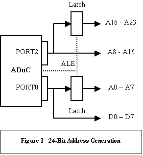
DMA conversion relies on three 8-bit pointers DMAL, DMAH, and DMAP to yield 24-bit pointer, which can be used to address 16 MByte of external data memory (SRAM). DMA operation still relies on two 8-bit ports Port0 and Port2 for addressing a 24-bit address space. Port0 on 8051 microcontroller places the lower order address lines (PA0-PA7) during the first part of external memory access, and this information is latched using an external IC (74HC573). ADuC812 extends this concept to multiplex the upper 8 address lines (A23-A16) with address. lines A15-A8 on Port2 This upper address lines are only necessary, if an external data space greater than 64K is required. In this case, the state of upper address lines can be latched by an external address latch IC.
The upper byte of address pointer DMAU is automatically incremented, whenever there is an overflow from DMAH during DMA operation. While reading from external data memory, under user software control, DMAU is automatically incremented upon an overflow from DPH. Thus the entire 16 MByte external data space can be utilized both for storage as well as for reading (from it) without the need for an external memory paging scheme.
Before DMA conversion can be initiated, it is necessary to set up the external data memory where the ADC results will be written. This requires
- Writing the channel # in upper nibble of memory location where high byte of ADC conversion result will be stored
- Writing a terminating sequence at the end of storage area.
The channel number has to be written for every single result of ADC conversion. Two bytes of external (8-bit) memory are required for storing conversion data. The DMA engine in ADuC812 stores the MSByte in lower memory and the LSByte in upper memory. Thus, the lower byte of every word location is written with the ADC channel to be converted. DMA engine uses the channel information provided in external memory to set the ADC multiplexer channels. Thus it is possible to use DMA controlled conversion for:
- Repeated conversion on one channel
- Sequential conversion on multiple channels set in order; such as ch 0 to ch 7
- Sequential conversion on multiple channels set in any random order; such as ch0, ch1, ch0, ch2, ch0, ch3, ch4, ch5, ch6, ch7, ch7, ch6, ch0, ch0 etc.
There is absolutely, no limitation on the order, in which the conversion need to be carried out. On practical side, however, the user will always have a certain order in mind.
Once, the external memory has been set up with information on the channel to be converted for the desired number of conversions, a terminating sequence needs to be written to external memory. The terminating sequence require that the information about last channel to be converted, is repeated one more time, followed by writing of value F0h in the next word location. DMA engine does not write the ADC result at the last repeated location, and leaves it unmodified.
The following example illustrate the process of setting up external memory for DMA operation.
Example 1: Set external memory for DMA controlled ADC conversion. The conversion to stop after the following four measurements. The channel conversion sequence is as follows:
Channel 1, Channel 2, Channel 1, Channel 3
Channel 1 is selected by writing 0001 to channel selection bit CS3, CS2, CS1, & CS0 in ADC control register ADCCON2. Similarly, selection bits for channel 2 are 0010 and 0011 for channel 3. This information needs to be written in MSBits of lower byte of each external memory (word) location. It is the location, where high byte of ADC result will be stored. The results are to be stored in external memory starting from 000000H.
The following program will set up this conversion sequence. It should be noted that the external memory set up will normally be done using the program loop, but this has been avoided to clearly show the program sequence.
MOV DMAL,#00H
MOV DMAH,#00H
MOV DMAL,#00H
MOV DPTR,#0000H ; Set DPTR to point to 0000 memory location
; Set first external memory location for ADC Ch 1
MOV A,#10H ; Load channel configuration CS3 CS2 CS1 CS0
MOVX @DPTR,A ; Store in XMEM where MSByte of result will be stored
INC DPTR ; Bump up pointer
CLR A
MOVX @DPTR,A ; Store 00 in XMEM LSByte of result (0) will be stored
; Set second external memory location for ADC Ch 2
INC DPTR
MOV A,#20H ; Channel configuration 0010
MOVX @DPTR,A ; XMEM, where MSByte of result (1) will be stored
INC DPTR ; Bump up pointer
CLR A
MOVX @DPTR,A ; XMEM, where LSByte of result (1) will be stored
; Set third external memory location for ADC Ch 1
INC DPTR
MOV A,#10H ; Channel configuration 0001
MOVX @DPTR,A ; XMEM, where MSByte of result (2) will be stored
INC DPTR ; Bump up pointer
CLR A
MOVX @DPTR,A ; XMEM, where LSByte of result (2) will be stored
; Set fourth external memory location for ADC Ch 3
INC DPTR
MOV A,#30H ; Channel configuration 0011
MOVX @DPTR,A ; XMEM, where MSByte of result (2) will be stored
INC DPTR ; Bump up pointer
CLR A
MOVX @DPTR,A ; XMEM, where LSByte of result (2) will be stored
; Set terminating sequence
; Repeat the last conversion command. Result from this conversion will not
; be stored.
INC DPTR
MOV A,#30H ; Repeat last channel configuration
MOVX @DPTR,A ; XMEM location for MSByte of result
INC DPTR ; Bump up pointer
CLR A
MOVX @DPTR,A ; XMEM location for LSByte of result
; Write ‘Stop’ command to terminate DMA operation
INC DPTR
MOV A,#0F0H ; Stop conversion command
MOVX @DPTR,A ; XMEM location for MSByte of result
END
The external memory contents after this initialization is shown in Table 4.
Table 4 Memory Contents After Initialization
Memory Adrs(Word) |
Contents
(binary) of Low Address |
Contents
(binary) of High Address |
ADC Conversion
Command |
|
000000 H |
0001 0000 |
0000 0000 |
Convert Ch 1 |
|
000002 H |
0010 0000 |
0000 0000 |
Convert Ch 2 |
|
000004 H |
0001 0000 |
0000 0000 |
Convert Ch 1 |
|
000008 H |
0011 0000 |
0000 0000 |
Convert Ch 3 |
|
00000A H |
0011 0000 |
0000 0000 |
Ch 3 (Dummy) |
|
00000C H |
1111 0000 |
XXXX XXXX |
Stop |
Once the external memory has been set up, DMA conversion mode is selected by setting ‘DMA’ bit in ADCCON2 control register (ADCCON2.6). When the ADC scan is complete, as dictated by initial data in external memory, an ADC conversion complete interrupt is generated setting the bit 0 (ADCI) in control register ADCCON2,
Digital Storage Scope
A very versatile digital storage scope (DSS) can be easily implemented using ADuC812. The following minimum components are needed for a DSS.
- ADuC812 with embedded DSS software
- Front-end Analogue buffer amplifier
- SRAM (32Kx8 or 128Kx8)
- Address latches (74HC573)
- RS-232 Buffer
- Voltage regulation circuit.
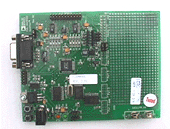
The ADuC812 QuickStart development system from Analog Devices contains all the above essential components. It contains a 32Kx8 SRAM, which is capable of storing 16,382 (16,384 – 2) measurements. This is a fairly large storage capacity and is sufficient for a basic digital storage scope. If, a larger capacity is desired additional SRAM (and associated logic) will need to be added to the development unit.
The complete DSS software consist of two parts:
- Embedded software running on ADuC812
- Mating software running on PC (or any other dedicated unit)
In this article, the discussion is limited to the embedded software needed to control ADuC812 operation.
ADuC812 Embedded DSS Software
The ADuC812 is operated in DMA mode, with ADC conversion rate controlled by Timer2. The conversion is limited to use channel 0 at this point. The user can control the sampling interval ranging from 10 usec to 20 msec and can store up to 4096 measurements. A fully commented source listing is provided. The embedded software operation can be summarized as follows:
- Initialize the ADuC812
- Get user input on the sampling rate
- Get user input on the number of channels
- Set up external memory for DMA control
- Set up DMA control mode
- Perform conversion
- Transmit the result to user.
All communication from and to ADuC812 is restricted to ASCII. Thus it is possible to even use a dump terminal or a PC running a terminal program to control ADuC812-DSS through keyboard and display the result on the user PC screen. The results are transmitted in groups of 16/line, with each result separated by a blank space.
Click here for Asm Source File
Happy
Digital Scoping
In the next issue
The mating PC Software will be discussed.
![]()
Reference:
- MicroConverter Data sheet, Analog Devices
- MicroConverter Product FAQs Analog Devices
- MicroConverter Application Notes, www.analog.com/MicroConverter
- MCS-51 Family of User’s Manual. Intel Corp, www.intel.com